Nikiforov
Vladimir O.
D.Sc., Prof.
doi: 10.17586/2226-1494-2016-16-6-1038-1047
DISTRIBUTION OF DISLOCATIONS IN AlN CRYSTALS GROWN ON EVAPORATING SiC SUBSTRATES
Read the full article
For citation: Argunova T.S., Gutkin M.Yu., Shcherbachev K.D., Kazarova O.P., Mokhov E.N., Jung Ho Je. Distribution of dislocations in AlN crystals grown on evaporating SiC substrates. Scientific and Technical Journal of Information Technologies, Mechanics and Optics, 2016, vol. 16, no. 6, pp. 1038–1047. doi: 10.17586/2226-1494-2016-16-6-1038-1047
Abstract
By the use of high-resolution X-ray diffractometry and synchrotron radiation topography, the distribution of dislocations in AlN crystals grown on evaporating SiC substrates is studied. The growth of AlN layer in one process with the evaporation of SiC substrate gave the possibility to prevent the relaxation of thermal stresses through cracking of AlN during cooling the structure. The continuous 0.2-1.5 mm thick plates were used as the model objects for the study of dislocation structure near the AlN/SiC interface. Analysis of the broadening of the Bragg reflection peaks, the shape of scattering maps in reciprocal space and topographs showed that dislocations formed the mosaic structure, different from the distribution of threading dislocations in GaN epilayers. A theoretical model for misfit strain relaxation in the growing AlN layer is suggested. The results enable to clarify the dislocation processes during sublimation growth of industrial quality AlN crystals.
Acknowledgements. M. Yu. Gutkin acknowledges the Russian Science Foundation (grant RSF No. 14-29-00086) for support in the development of a theoretical model of misfit stress relaxation in AlN crystals, and E. N. Mokhov acknowledges the Russian Science Foundation (grant RSF No. 16–42–01098) for support in carrying out experimental research.
References
1. Brandt O., Muralidharan R., Waltereit P., Thamm A., Trampert A., von Kiedrowski H., Ploog K.H. Critical issues for the growth of high-quality (Al,Ga)N/GaN and GaN/(In,Ga)N heterostructures on SiC(0001) by molecular-beam epitaxy. Applied Physics Letters, 1999, vol. 75, no. 25, pp. 4019–4021.
2. Kyutt R.N., Ratnikov V.V., Mosina G.N., Shcheglov M.P. Structural perfection of GaN epitaxial layers according to x-ray diffraction measurements. Physics of the Solid State, 1999, vol. 41, no. 1, pp. 25–31.
3. Lee C.D., Ramachandran V., Sagar A., Feenstra R.M., Greve D.W., Sarney W.L., Salamanca-Riba L., Look D.C., Bai S., Choyke W.J., Devaty R.P. Properties of GaN epitaxial layers grown on 6H-SiC(0001) by plasma-assisted molecular beam epitaxy. Journal of Electronic Materials, 2001, vol. 30, no. 3, pp. 162–169.
4. Heying B., Wu X.H., Keller S., Li Y., Kapolnek D., Keller B.P., DenBaars S.P., Speck J.S. Role of threading dislocation structure on the x-ray diffraction peak widths in epitaxial GaN films. Applied Physics Letters, 1996, vol. 68, no. 5, pp. 643–645. doi: 10.1063/1.116495
5. Kapolnek D., Wu X.H., Heying B., Keller S., Keller B.P., Mishra U.K., DenBaars S.P., Speck J.S. Structural evolution in epitaxial metalorganic chemical vapor deposition grown GaN films on sapphire. Applied Physics Letters, 1995, vol. 67, no. 11,pp. 1541–1543. doi: 10.1063/1.114486
6. Nagai I., Kato T., Miura T., Kamata H., Naoe K., Sanada K., Okumura H. AlN bulk single crystal growth on 6H-SiC substrates by sublimation method. Journal of Crystal Growth, 2010, vol. 312, no. 19, pp. 2699–2704. doi: 10.1016/j.jcrysgro.2010.05.044
7. Sumathi R.R. Bulk AlN single crystal growth on foreign substrate and preparation of free-standing native seeds. CrystEngComm, 2013, vol. 15, no. 12, pp. 2232–2240. doi: 10.1039/c2ce26599k
8. Sumathi R.R., Barz R.U., Straubinger T., Gille P. Structural and surface topography analysis of AlN single crystals grown on 6H-SiC substrates. Journal of Crystal Growth, 2012, vol. 360, no. 1, pp. 193–196. doi: 10.1016/j.jcrysgro.2011.11.054
9. Argunova T.S., Gutkin M.Yu., Mokhov E.N., Kazarova O.P., Lim J.-H., Scheglov M.P. Prevention of AlN crystal from cracking on SiC substrates by evaporation of the substrates. Physics of the Solid State, 2015, vol. 57, no. 12, pp. 2473–2478. doi: 10.1134/S1063783415120057
10. Argunova T.S., Gutkin M.Yu., Kazarova O.P., Mokhov E.N., Nagalyuk S.S., Je J.H. Synchrotron x-ray study on crack prevention in AlN crystals grown on gradually decomposing SiC substrates. Materials Science Forum, 2015, vol. 821–823, pp. 1011–1014. doi: 10.4028/www.scientific.net/MSF.821-823.1011
11. Mokhov E., Izmaylova I., Kazarova O., Wolfson A., Nagalyuk S., Litvin D., Vasiliev A., Helava H., Makarov Y. Specific features of sublimation growth of bulk AlN crystals on SiC wafers. Physica Status Solidi C, 2013, vol. 10, no. 3, pp. 445–448. doi: 10.1002/pssc.201200638
12. Srikant V., Speck J.S., Clarke D.R. Mosaic structure in epitaxial thin films having large lattice mismatch. Journal of Applied Physics, 1997, vol. 82, no. 9, pp. 4286–4295.
13. Sumathi R.R., Barz R.U., Gille P., Straubinger T. Influence of interface formation on the structural quality of AlN single crystals grown by sublimation method. Physica Status Solidi C, 2011, vol. 8, no. 7–8, pp. 2107–2109. doi: 10.1002/pssc.201000941
14. Floro J.A., Follstaedt D.M., Provencio P., Hearne S.J., Lee S.R. Misfit dislocation formation in the AlGaN/GaN heterointerface. Journal of Applied Physics, 2004, vol. 96, no. 1, pp. 7087–7094. doi: 10.1063/1.1812361
15. Miyanaga M., Mizuhara N., Fujiwara S., Shimazu M., Nakahata H., Kawase T. Evaluation of AlN single-crystal grown by sublimation method. Journal of Crystal Growth, 2007, vol. 300, pp. 45–49. doi: 10.1016/j.jcrysgro.2006.10.233
16. Bickermann M., Epelbaum B.M., Filip O., Heimann P., Nagata S., Winnacker A. Structural properties of aluminum nitride bulk single crystals grown by PVT. Physica Status Solidi C, 2008, vol. 5, pp. 1502–1504. doi: 10.1002/pssc.200778422
17. Kamata H., Naoe K., Sanada K., Ichinose N. Single-crystal growth of aluminum nitride on 6H-SiC substrates by an open-system sublimation method. Journal of Crystal Growth, 2009, vol. 311, no. 5, pp. 1291–1295. doi: 10.1016/j.jcrysgro.2008.12.025
PICTURES

Fig.1 X-ray topograms obtained in the synchrotron radiation from AlN crystal with evaporated SiC substrate. Polychromatic radiation. Laue geometry. Kodak M100 film. Images of borders seem double, because the emulsion layer has been coated on both sides of the film (a). Monochromatic radiation with energy E = 20 keV. Bragg geometry. CCD detector with pixel size equal to 16 µm (b, c)

Fig.2. Triple-crystal intensity distribution curves depending on wangle measured by w- and 2q–w-scanning in 0004 reflection from AlN crystal with evaporated substrate. Ww= 114 arcsec., W2q–w = 110 arcsec. Approximation of peaks by Gaussian and Voigt functions is shown with dashed and solid lines, respectively

a)

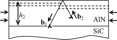
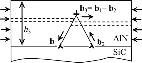
Fig. 3. The scheme of possible mechanisms of misfit stress relaxation when growing the single crystal AlN layer on the evaporating SiC substrate. The initial relaxation stage due to nucleation of the moving dislocation half-loops on compressed AlN layer surface with thickness, much smaller than the thickness of the substrate (a). The final relaxation stage by the formation of L-shaped dislocation configurations in the AlN layer allowing for misfit stress relaxation both near and away from AlN/SiC interface (b). The inserts schematically show misfit stress diagrams in the cross section of the structure and pyramidal slip plane in AlN layer

a)

b)

c)

d)

e)
Fig. 4. A theoretical model of L-shaped dislocation configuration appearance near AlN/SiC interface. The initial state of plane coherent AlN layer with thickness h much less than the thickness of SiC substrate (a). The nucleation of a dislocation half-loop with Burger's vector b1, moving along pyramidal slip plane in the direction from AlN layer surface to AlN/SiC interface at h=hc (b). Surface step becomes overgrown and changes its face on mirror-symmetric one with h=h1>hc; the tilted line segment of b1-dislocation becomes overgrown from this face to AlN/SiC interface. The dashed line shows the position of AlN layer surface for h=hc (c). On the surface step "secondary" dislocation half-loop is nucleated with Burger's vector b2, and it slides symmetrically relative to b1-dislocation half-loop from AlN layer surface to AlN/SiC interface at h=h2>h1. As a result, the surface step disappears, and L-shaped dislocation configuration begins to be formed. The dashed lines show the locations of AlN layer surface for h=hcand h=h1 (d). End L-shaped dislocation configuration with an upper dislocation segment with Burger's vector b3=-b1-b2 and closing half-loops of b1 - and b2-dislocations, with h=h3>h2 (e)


